
Solid State Drive Primer # 6 - NAND Architecture - Component Packaging
 Previous articles on the NAND architecture started at the basic NAND cell and built up to the NAND die level. We go up one more level in this article to discuss common NAND component packaging options.
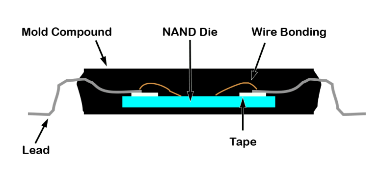
The NAND die themselves are relatively fragile and require special equipment for placement and bonding. Typically NAND die are placed inside a protective component package as opposed to directly on a circuit board. Most follow an open industry standard defined by JEDEC.
These components allow a manufacturer to place a single or several NAND die inside one package with a standard pin-out of typically a TSOP or BGA package. The standard packages are easily handled by the pick and place systems as they adhere the parts to printed circuit boards (PCBs) prior to being run through soldering machines.
BGA Packaged NAND
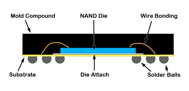

There is an insulating layer between each NAND die and connections are made from each NAND die to the substrate using a wire bonding machine. The substrate is like a very thin PCB (Printed Circuit Board) which is the base for the stacked die. As with the single die cutaway shown earlier, the entire top of the component is encapsulated.
If the parts share a JEDEC standard form factor, the parts appear physically identical regardless of the number of die inside.
TSOP Packaged NAND
Future articles will look at putting the NAND components and a controller together to create a Solid State Drive as well as the challenges required of the SSD controller technology.
If you would like to discuss this further please contact us.

Your article helped me a lot, is there any more related content? Thanks!
Thank you for your sharing. I am worried that I lack creative ideas. It is your article that makes me full of hope. Thank you. But, I have a question, can you help me?
Thank you for your sharing. I am worried that I lack creative ideas. It is your article that makes me full of hope. Thank you. But, I have a question, can you help me?
Thanks for sharing. I read many of your blog posts, cool, your blog is very good.
Your article helped me a lot, is there any more related content? Thanks!
Your point of view caught my eye and was very interesting. Thanks. I have a question for you.
I don't think the title of your article matches the content lol. Just kidding, mainly because I had some doubts after reading the article.
Your point of view caught my eye and was very interesting. Thanks. I have a question for you.
Your article helped me a lot, is there any more related content? Thanks!
Thanks for sharing. I read many of your blog posts, cool, your blog is very good.
Your point of view caught my eye and was very interesting. Thanks. I have a question for you.
I don't think the title of your article matches the content lol. Just kidding, mainly because I had some doubts after reading the article.
Your point of view caught my eye and was very interesting. Thanks. I have a question for you.
Can you be more specific about the content of your article? After reading it, I still have some doubts. Hope you can help me.
Your point of view caught my eye and was very interesting. Thanks. I have a question for you.
I don't think the title of your article matches the content lol. Just kidding, mainly because I had some doubts after reading the article.
Thank you for your sharing. I am worried that I lack creative ideas. It is your article that makes me full of hope. Thank you. But, I have a question, can you help me?
Thanks for sharing. I read many of your blog posts, cool, your blog is very good.
Thank you for your sharing. I am worried that I lack creative ideas. It is your article that makes me full of hope. Thank you. But, I have a question, can you help me?
Thank you for your sharing. I am worried that I lack creative ideas. It is your article that makes me full of hope. Thank you. But, I have a question, can you help me? https://www.binance.com/futures/ref?code=JW3W4Y3A
Great breakdown of NAND packaging — wire bonding and BGA substrates are key to reliability. Also I use nanobanana2
for quick component architecture diagrams.