
Poor SSD Controller Design Compromises the Best NAND Memory
Let’s take a look at the three major areas which comprise a solid state drive.
- NAND Memory Type and Trace Width Geometry
- Controller Architecture, Firmware Algorithms
- Physical Construction, Ancillary Components, PCB, etc.
NAND Memory Type and Trace Width Geometry
NAND memory is available in several types today. Each has its advantages and disadvantages as shown in the table below.
| NAND TYPE | ADVANTAGES | DISADVANTAGES |
|---|---|---|
| SLC (SINGLE LEVEL CELL) |
UP TO 70,000 ENDURANCE CYCLES PER PHYSICAL BLOCK | HIGH COST |
| MLC (MULTI LEVEL CELL) |
2000 - 3000 ENDURANCE CYCLES PER PHYSICAL BLOCK | MEDIUM COST, ONLY AVAILABLE IN FINER TRACE WIDTHS, SHORT LIFE CYCLE |
| TLC (TRI LEVEL CELL) |
LOW COST | AS LOW AS 200 - 300 ENDURANCE PER PHYSICAL BLOCK |
As you can see there are options to fit reliability and cost budgets. With all of these options, it’s no coincidence there is confusion in the market.
The vast majority of the flash storage market is focused on consumer electronics, client PCs and enterprise storage solutions which value performance and cost more than reliability. For this market, TLC NAND based solid state storage systems based on the finest geometry trace width provide the low-cost criteria necessary at the expense of reliability.
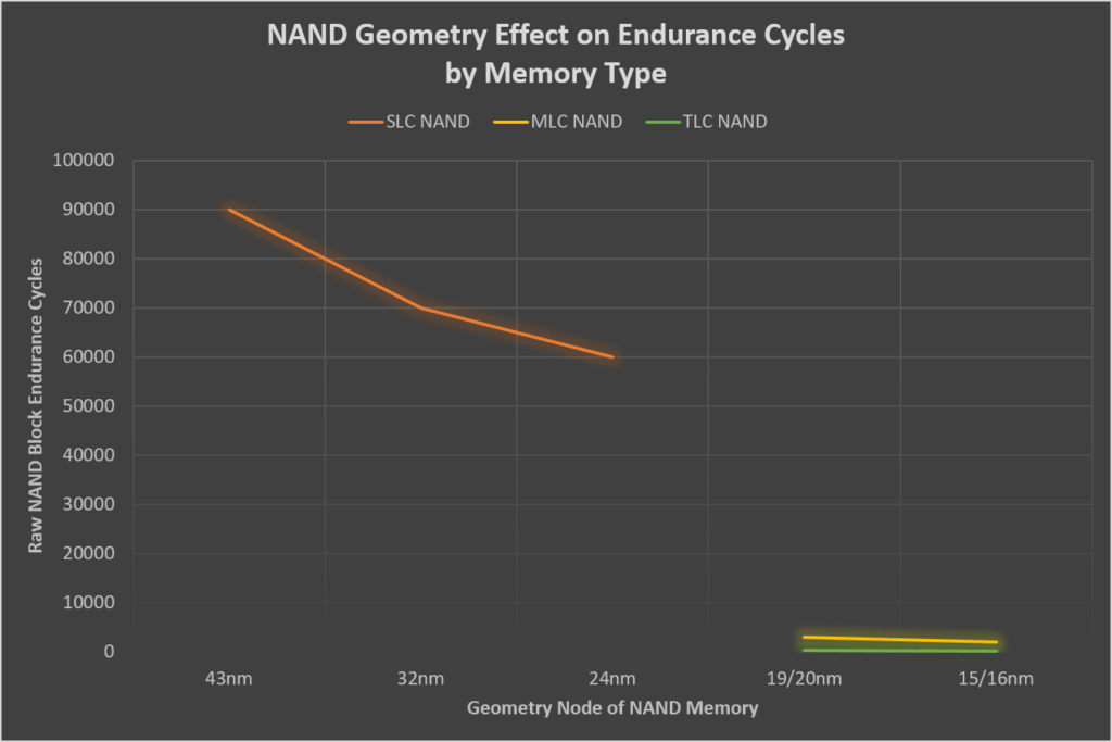
The chart below shows the significant differences in the number of raw Endurance cycles per physical block of NAND Flash memory based on NAND Flash type and the Geometry Node of its fabrication.
Two other derivatives of the three main memory types are pSLC and eMLC NAND memory. A future article will dig deeper into these technologies, but a brief explanation is below:
pSLC - Pseudo Single Level Cell - As the pseudo in the name suggests, this is NOT SLC NAND. It is a MLC NAND component being used as 1-bit per cell versus its normal 2-bit per cell operation.
Since only half the capability of each cell is used, only half the total MLC NAND’s capacity is available (ex: 32GB MLC NAND is only usable as 16GB).
Using MLC NAND in the pSLC configuration does NOT make it as reliable as a SLC NAND component. The MLC NAND is made from a much smaller geometry node and has the associated issues with endurance and ECC errors. There is not substantial data to back up pSLC as any more reliable than using the full capacity of the MLC component with 2x the cells to perform wear leveling.
eMLC - Enterprise Multi Level Cell - This is a sorted MLC component which has its endurance increased from typical 2000-3000 cycles to 10,000-20,000 cycles. The tradeoff is a lower data retention of about 30 days as well as a price premium.
Neither the pSLC or eMLC NAND memory has made significant inroads to the Embedded OEM market. They tend to be focused on the Enterprise SSD market in which the SSD acts more like a cache than a long term storage device.
Geometry Node (aka Trace Width) has a profound effect on the endurance of NAND memory cells of all types. Endurance is a key, but not the only factor when considering reliability of NAND devices. As Geometries get smaller, error rates become an increasing issue due to the closer proximity of neighboring cells in the NAND silicon.
Initial testing of MLC NAND and finer trace width SLC NAND memory is ongoing. As the trace widths decrease, reliability decreases as well. We will continue to publish our findings as they become available.
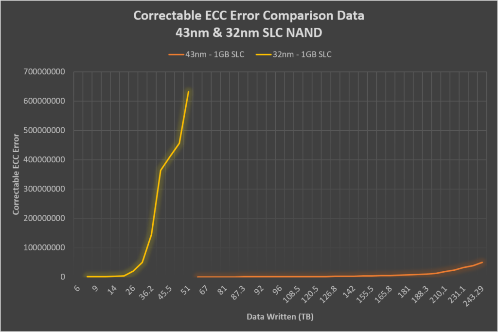
All NAND devices will have errors during use, this is due to a variety of factors - charge leakage, sense amp. errors, disturbance due to noise coupling, device wear out, etc. That's why all flash controllers incorporate ECC hardware to correct these errors on the fly.
ECC hardware has a fixed correction capability; as the device wears out and error rate increases, it will eventually overwhelm the ECC correction capability and cause device failure. Lower error rates are better for long term reliability.
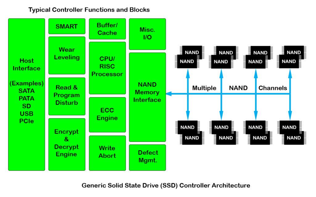
Controller Architecture, Firmware Algorithms
 Controller architecture and firmware algorithms play an important role in the reliability, performance and cost of a solid state drive device. A Consumer controller paired with the most reliable 43nm SLC NAND flash, will cause issues since the controller is the weak link in the chain.
An Industrial Grade controller, with reliable architecture and firmware algorithms are key. Here are a few points which differentiate Industrial reliability from Consumer and Enterprise SSD:
- DRAM-less Design – DRAM cache increases probability of data corruption during sudden power loss event.
- Read Disturb Management – shrinking NAND geometries increases the likelihood of read disturb errors (i.e. frequent reads can cause bit errors due to inter-cell noise coupling); Cactus Technologies latest generation industrial grade products (e.g. 503, 900S, 808) include Read Disturb Management features since they use the finer 32nm SLC NAND components.
- Robust Power-Fail Protection – firmware architecture is designed to be able to always recover the last valid state; firmware is robustly tested through power cycling tests.
- On-the-fly Garbage Collection – many flash products do garbage collection during IDLE time to maximize performance when the device is active; however, this increase the likelihood of write abort data corruption as the host system may remove power during IDLE time while the device is still doing program/erase operations internally. Cactus Technologies industrial grade products performs on-the-fly garbage collection; while this will reduce performance slightly, it ensures that the host can safely power down the device during IDLE time.
Physical Construction, Ancillary Components, PCB, etc.
The final piece of the puzzle is how the device is physically constructed and what non-controller or NAND memory components are used.
Key differentiators for Industrial Grade products in this area are:
- Strong, Die Cast Metal Chassis instead of weak, plastic chassis for SSD products
- True Industrial Grade NAND instead of commercial grade NAND that may or may not have been temperature screened
- At the recent Embedded World show we were told of NAND components from recycled Smart Phones being built into new SSD after completing NAND die testing. There is no way to determine how many endurance cycles had already been consumed.
- High Quality 4-8 Layer PCB for superb signal integrity
- For Extended -45C to 90C operating temperature devices, all components used are rated for industrial temperature range.
In addition to these items, long life cycles, Locked BOM, service and support should also be considered when choosing a supplier for your Embedded OEM application.
Please contact us for more details if your OEM design requires flash storage.

I don't think the title of your article matches the content lol. Just kidding, mainly because I had some doubts after reading the article.
I don't think the title of your article matches the content lol. Just kidding, mainly because I had some doubts after reading the article.
Your point of view caught my eye and was very interesting. Thanks. I have a question for you.
I don't think the title of your article matches the content lol. Just kidding, mainly because I had some doubts after reading the article.
Your point of view caught my eye and was very interesting. Thanks. I have a question for you.
Your article helped me a lot, is there any more related content? Thanks!
Your point of view caught my eye and was very interesting. Thanks. I have a question for you.
Your point of view caught my eye and was very interesting. Thanks. I have a question for you.
I don't think the title of your article matches the content lol. Just kidding, mainly because I had some doubts after reading the article.
Thanks for sharing. I read many of your blog posts, cool, your blog is very good.
Can you be more specific about the content of your article? After reading it, I still have some doubts. Hope you can help me.
Can you be more specific about the content of your article? After reading it, I still have some doubts. Hope you can help me.
Can you be more specific about the content of your article? After reading it, I still have some doubts. Hope you can help me.
Your article helped me a lot, is there any more related content? Thanks! https://www.binance.info/es-MX/register-person?ref=JHQQKNKN
Thank you for your sharing. I am worried that I lack creative ideas. It is your article that makes me full of hope. Thank you. But, I have a question, can you help me? https://www.binance.info/de-CH/register?ref=UM6SMJM3
Your point of view caught my eye and was very interesting. Thanks. I have a question for you.
I don't think the title of your article matches the content lol. Just kidding, mainly because I had some doubts after reading the article.
Thanks for sharing. I read many of your blog posts, cool, your blog is very good. https://www.binance.info/da-DK/register?ref=V3MG69RO
Can you be more specific about the content of your article? After reading it, I still have some doubts. Hope you can help me. https://www.binance.info/register?ref=JW3W4Y3A