
Solid State Drive Primer # 9 - Controller Architecture - Controller Block Diagram
 This article follows the Controller Architecture article on NAND Channels and Banks. It will focus on the main blocks of a generic SSD controller and its connection to the NAND flash. Controller functionality varies with the type of product it is intended for.
A simple consumer SD card controller is designed for cost and in some cases performance. For this application, it would be an overkill and unneeded expense to add an encryption & decryption engine to the silicon.
In other cases, such as secure military grade SSD, encryption & decryption are an absolute necessity. Other applications rely on SMART data to predict an imminent failure looming in the future so the SSD can be replaced prior to an unexpected failure.
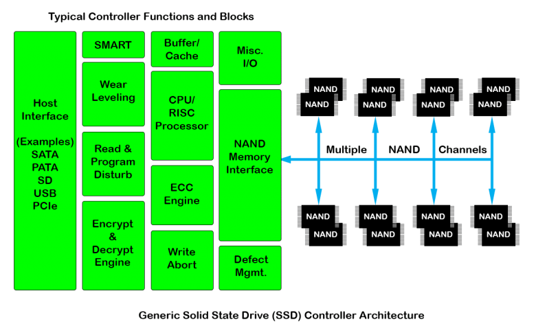
Host Interface:
 The host interface of a controller is typically designed to one specific interface specification. There are several interfaces made to address different system and design requirements. The most popular are SATA, SD, USB, PATA/IDE and PCIe.
SMART (Self-Monitoring, Analysis and Reporting Technology):
 The SMART function, available in some controllers, monitors and records data regarding many attributes of the SSD and memory. An example is the ability to monitor the percentage of endurance cycles remaining in the SSD since this is a key determining factor of the life remaining.
Wear Leveling:
 Wear Leveling is the ability to even out the number of write cycles throughout the available NAND. Since each NAND block has a limited number of erase/write cycles, if only one physical block is written continuously, it will quickly deplete its endurance cycles. A controller’s Wear Leveling algorithm monitors and spreads out the writes to different physical NAND blocks.
Read & Program Disturb:
 With the finer and finer trace widths of the NAND flash, more issues arise to maintain the data contents of the NAND cells. Read & Program Disturb occur when cells are read or written causing cross coupling to adjacent cells and occasionally changing their values. Controllers need algorithms and in some cases circuitry to compensate for this phenomena.
Encrypt & Decrypt Engine:
 For higher security applications, a hardware encryption and decryption engine is generally built into the silicon of the controller. The encryption engine is typically implemented in hardware to ensure speed for encrypting/decrypting on the fly. The most popular encryption method for SDDs today is AES256.
Buffer/Cache:
 Controllers generally have a high speed SRAM/DRAM cache buffer used for buffering the read and/or write data of the SSD. Since this cache uses volatile memory, it subjects data to loss if power is unexpectedly lost. It is common to see both internal caches in the controller chip itself as well as external cache chips.
CPU/RISC Processor:
ECC Engine:
 Error Checking & Correction are a key part of today’s SSD. ECC will correct up to a certain number of bits per block of data. Without ECC, many of the low cost consumer flash cards using very inexpensive memory would not be possible.
Write Abort:
 Write Abort is the when power to the SSD is lost during a write to the NAND flash. Without a battery or SuperCap backed cache, it is likely this data in transit will be lost. The more important aspect of this is to ensure the SSD’s internal metadata and firmware remain uncorrupted. This is the function of Write Abort circuitry mainly found in Industrial Grade products.
Miscellaneous I/O:
 Simple functions such as chip select pins for the NAND components are handled with several input/output pins. There are also a number IO functions required for initial programming and production.
NAND Memory Interface:
 The NAND memory interface was covered in the previous article on NAND banks and channels. Depending on the controller there can be a single NAND channel up to 10 or more. Each channel can have one or more NAND chips.
Defect Management:
 Every controller needs a method to deal with bad blocks of memory and new defects. At the point a NAND block becomes unusable, some action on the SSD controller’s part must happen. In some cases a spare sector replaces the failed block. In a poor controller design, the SSD fails. Each controller has its method to deal with defects.The next article will hit on some bigger picture common issues and methods SSDs use to address them.
If you would like to discuss this further please contact us.

Your article helped me a lot, is there any more related content? Thanks!
Your article helped me a lot, is there any more related content? Thanks!
Thanks for sharing. I read many of your blog posts, cool, your blog is very good.
Thank you for your sharing. I am worried that I lack creative ideas. It is your article that makes me full of hope. Thank you. But, I have a question, can you help me?
Your article helped me a lot, is there any more related content? Thanks!
Thank you, your article surprised me, there is such an excellent point of view. Thank you for sharing, I learned a lot.
I don't think the title of your article matches the content lol. Just kidding, mainly because I had some doubts after reading the article.
Thank you for your sharing. I am worried that I lack creative ideas. It is your article that makes me full of hope. Thank you. But, I have a question, can you help me?
I don't think the title of your article matches the content lol. Just kidding, mainly because I had some doubts after reading the article.
Can you be more specific about the content of your article? After reading it, I still have some doubts. Hope you can help me.
Thanks for sharing. I read many of your blog posts, cool, your blog is very good.
Thanks for sharing. I read many of your blog posts, cool, your blog is very good. https://www.binance.info/register?ref=IHJUI7TF
Can you be more specific about the content of your article? After reading it, I still have some doubts. Hope you can help me.
Thanks for sharing. I read many of your blog posts, cool, your blog is very good. https://www.binance.info/register?ref=IHJUI7TF
I don't think the title of your article matches the content lol. Just kidding, mainly because I had some doubts after reading the article.
Thanks for sharing. I read many of your blog posts, cool, your blog is very good. https://accounts.binance.com/register-person?ref=IXBIAFVY
Your point of view caught my eye and was very interesting. Thanks. I have a question for you.
Can you be more specific about the content of your article? After reading it, I still have some doubts. Hope you can help me.
Can you be more specific about the content of your article? After reading it, I still have some doubts. Hope you can help me.
I don't think the title of your article matches the content lol. Just kidding, mainly because I had some doubts after reading the article.
Your point of view caught my eye and was very interesting. Thanks. I have a question for you.
Thank you for your sharing. I am worried that I lack creative ideas. It is your article that makes me full of hope. Thank you. But, I have a question, can you help me?
I don't think the title of your article matches the content lol. Just kidding, mainly because I had some doubts after reading the article. https://www.gate.com/share/XwNAUwgM
Thanks for sharing. I read many of your blog posts, cool, your blog is very good.
I don't think the title of your article matches the content lol. Just kidding, mainly because I had some doubts after reading the article.
Your point of view caught my eye and was very interesting. Thanks. I have a question for you. https://accounts.binance.bh/register/person?ref=GGYHGRE