Solid State Drive Primer # 1 - The Basic NAND Flash Cell
 This article takes a look at the basics of a NAND flash cell, the building block of almost every solid state drive. It is the first of several articles that will describe the basics of Solid State Drives (SSD).
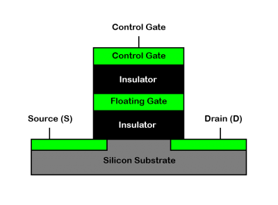
In order to store a single bit of data on a solid state drive, you need the smallest building block - a single NAND flash cell. The simplest NAND cell can be set to either a 0 or 1 state. It will continue to store that state even after power has been removed.
What does a NAND Cell look like?
In its simplest form when the floating gate is charged, it is programmed and recognized as a binary 0. When the floating gate has no charge it is erased and recognized as a binary value of 1.
| FLOATING GATE STATE | REFERRED TO AS | BINARY VALUE ASSIGNED |
|---|---|---|
| CHARGED | PROGRAMMED | ZERO - 0 |
| NO CHARGE | ERASED | ONE - 1 |
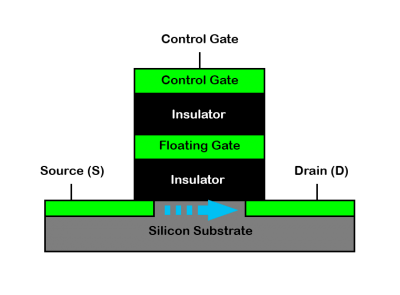
How to Read a NAND Cell:
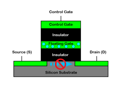
If there is no current flow, it signifies the floating gate is charged (binary 0) - as in the diagram above. If there is current flow, the floating gate is not charged (binary 1) - as in the diagram below.
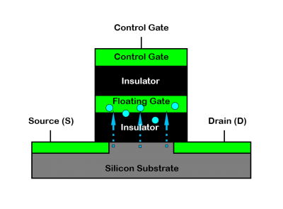
How to Write a NAND Cell:
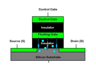
To write a cell, a high voltage is applied to the control gate and electrons move from the silicon substrate to the floating gate. This process is called tunneling since the electrons “tunnel” through the oxide insulator to reach the floating gate. See diagram below.
How to Erase a NAND Cell:
To erase a NAND cell, a high voltage is applied to the silicon substrate and electrons move from the floating gate to the silicon substrate. This uses the same tunneling process as the writing process. See diagram below.
NAND Cell life:
The tunneling process described in the Write and Erase functions above cause stress on the oxide insulator layer. Over time this stress breaks down the oxide layer and the floating gate becomes unable to maintain a charge. At some point the cell is no longer usable and must be retired. This is what is responsible for the finite number of writes/erases per cell of NAND flash.
If you would like to discuss further, please contact us.